
Short Answer
A transistor is a three-terminal semiconductor device that uses a small control signal to regulate a larger current path. A bipolar junction transistor (BJT) uses base current in the circuit model. A metal-oxide-semiconductor field-effect transistor (MOSFET) responds to gate voltage measured relative to its source. A transistor circuit can amplify variations in a signal or switch a load between commanded off and on states.
The control input and the load path have different jobs. An amplifier holds the device at an operating point where changes at the input produce a larger, corresponding output signal. The output may be inverted, depending on where it is taken. A switch drives the device toward either end of its operating range. In both cases, the supply provides the energy that reaches the load.
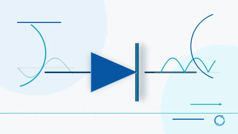
From a Diode to a Three-Terminal Device
A diode’s forward and reverse behavior follows the voltage between its two terminals. A BJT adds a control terminal, the base, which is shared by its two PN junctions. One junction sits between base and emitter, and the other between base and collector. That arrangement lets a base input affect the current in a separate collector path. The forward voltage of the base-emitter junction is a useful connection back to how a diode works.
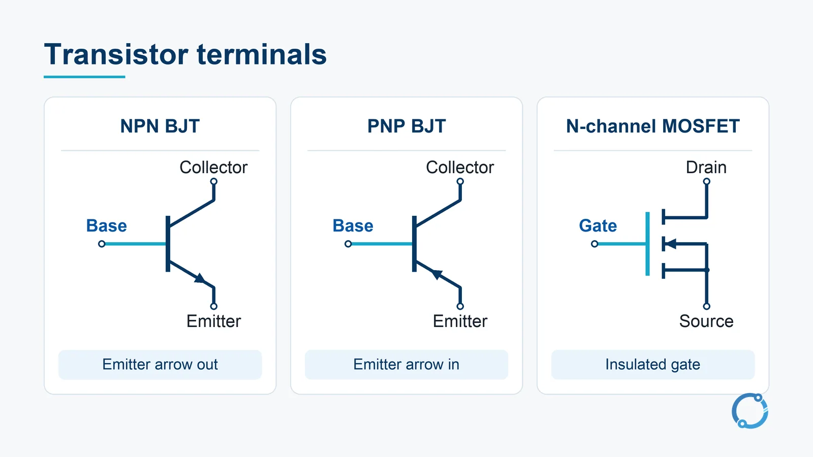
In a BJT symbol, the slanted lead with the arrow is the emitter. An NPN transistor has an emitter arrow pointing away from the base line. A PNP transistor has an emitter arrow pointing toward it. The other slanted lead is the collector. The straight lead into the base line is the base. Use the arrow and the terminal labels even when the symbol is rotated in a drawing. MIT’s BJT notes show both symbol orientations and their current directions.
A MOSFET has a gate, drain and source in the three-terminal form shown here. The small gap beside the gate line represents insulation. The drain and source are the ends of the controlled channel. The drawing uses an enhancement-mode N-channel symbol with the body tied to the source. Other common drawings simplify that connection. Each schematic symbol describes electrical roles. The actual order of physical pins depends on the device. Purdue’s MOSFET lecture shows common symbol variants.
How an NPN BJT Controls Collector Current
An NPN BJT conducts in its forward-active region when the base-emitter junction is forward biased and the base-collector junction remains reverse biased. In a first-pass silicon circuit calculation, the forward base-emitter drop, VBE, is often taken as about 0.7 V. This is a typical working approximation. The actual drop changes with current and temperature.
In this region, a simple current model is IC ≈ β × IB, where IC is collector current, IB is base current and β is the DC current gain at the operating point. With the ordinary NPN current directions, the collector and base currents enter the device and add at the emitter, so IE = IC + IB. The current gain varies from device to device and with collector current and temperature. The emitter-current balance still applies when the forward-active gain approximation stops applying.
The base circuit establishes the drive, while the collector circuit needs a supply and a load path to support the predicted current. A resistor in the collector leg also turns changes in collector current into changes in voltage. A larger collector current increases the drop across that resistor, pulling the collector voltage down. That is the origin of the inversion in the common-emitter amplifier shown later.
Worked Example 1: Forward-Active Current Gain
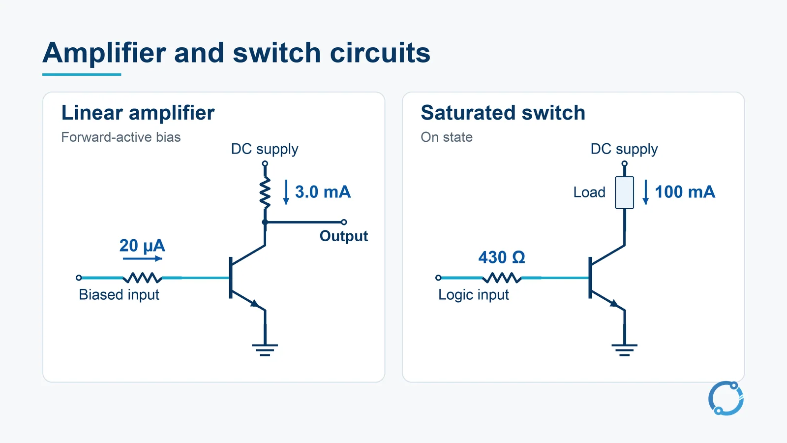
Assume a base current of 20 µA and take β = 150 as a typical illustrative value at the chosen forward-active operating point. The estimate is IC = 20 µA × 150 = 3.0 mA. The collector circuit must leave enough voltage across the transistor for it to stay forward active at that current. This is a current estimate at the assumed bias point. Voltage gain depends on the surrounding amplifier circuit.
A PNP BJT mirrors the usual NPN voltage and current directions. Its emitter sits at a higher potential than its base during forward drive. Conventional current enters the emitter and leaves through the collector and base. The same current-gain relationship can be written using current magnitudes in the active region. The reversed arrow keeps those reference directions visible on the schematic.
Cutoff, Forward Active and Saturation in a BJT
The circuit around a BJT determines which operating region it occupies. For a switch, the useful endpoints are cutoff and saturation. For a linear amplifier, the intended signal swing stays within the forward-active region. Like a valve, the device can vary the flow or be driven toward either endpoint.
Cutoff is the off state. With the base-emitter junction driven below meaningful forward conduction under the circuit’s normal conditions, collector current falls to a small leakage level. In a low-side switch with the load tied to a positive supply, the open current path leaves the load effectively off and lets the collector sit near the supply voltage.
Forward active is the amplification region. Bias establishes a steady point so that the input can move in either direction around it. Over a suitable swing, the collector responds to the changing input. A signal driven too far toward cutoff or saturation will clip at that end of the swing. The setting of the bias and the available collector voltage therefore matter as much as the fact that a BJT can provide current gain.
Saturation is the on state for the BJT switch. With adequate base drive, both junctions are forward biased and the collector-emitter voltage is low. It retains a finite on-state drop. The supply and load largely determine the collector current once the transistor has reached that state. Trace the load and switch as one current path using the series and parallel circuit rules. The base drive feeds a separate branch that returns through the emitter.
Worked Example 2: Base Drive for a Saturated Switch
Suppose the load requires IC = 100 mA. Select a forced β of 10 for this teaching example. Forced β is the chosen ratio of load current to available base current in the intended on state. The required base drive is IB = 100 mA ÷ 10 = 10 mA.
Assume the driver’s high output stays at 5 V while supplying that base current and use VBE ≈ 0.7 V for the forward junction. The base resistor sees the difference between those voltages. With the current expressed in amps, RB = (5 V − 0.7 V) ÷ 0.010 A = 430 Ω.
Switch design deliberately derates the gain used to budget base drive. A forced ratio around one tenth of a suitable active-region gain reference can be a starting rule of thumb. Here the forced ratio of 10 is a separate assumption and makes the base drive one tenth of the intended collector current. The β of 150 belongs to the amplification example. Driving the base harder than an active-region current estimate would suggest helps put the BJT into saturation with the specified load. Auburn University’s switching lab demonstrates the forced-beta check.
For a real circuit, check the specified saturation conditions for the intended collector current, base current and temperature. Also check the high level the driver actually maintains under load and use the applicable base-emitter voltage. A driver that sags supplies less base current through the resistor. If the BJT remains forward active when commanded on, more voltage can stay across it, leaving less for the load and increasing transistor dissipation. The calculated 430 Ω follows the stated assumptions.
How a MOSFET Controls the Drain-to-Source Path
A MOSFET responds to its gate-to-source voltage, VGS. Always use the source as the reference when deciding whether the gate drive is sufficient. For an enhancement-mode N-channel device, driving the gate sufficiently positive relative to the source creates a conducting channel. Returning the gate to source potential turns the controlled channel off. A P-channel enhancement device uses the mirrored polarity, with its gate driven below its source to turn on.
The insulated gate draws very little steady DC current. Current still flows into or out of the gate while its voltage changes because the gate has capacitance. A driver therefore has to transfer charge during each transition. With a weak driver, the MOSFET spends longer passing through intermediate conduction, where it can carry noticeable current while still dropping voltage.
Gate threshold describes the onset of conduction under stated test conditions. For switching a load, look at the gate voltage for which the manufacturer specifies the drain-to-source on-resistance, RDS(on). A well-enhanced MOSFET behaves approximately like a small resistance along its conducting path. At a given on-resistance, conduction heating scales as I² × RDS(on), where I is the drain current. The relevant resistance depends on gate drive and temperature. MIT’s switch lecture explains the on-resistance and gate-charge distinction.
The word “saturation” shifts meaning between the device families. In a BJT switch, it identifies the low-drop on state. In MOSFET terminology, saturation describes an operating region often used in amplification. The fully enhanced MOSFET switch normally operates in the low-resistance ohmic region. The useful check for a switch is the voltage or resistance left in the power path at the intended load current.
Where IGBTs Fit
An insulated-gate bipolar transistor (IGBT) combines a MOS-controlled insulated gate with bipolar conduction in the output path. The control input acts through gate voltage while the output path carries the power current. In a variable frequency drive, IGBTs can be the power-stage switches that shape the motor supply. In an inverter, they can switch the DC link to form the output waveform. UCF’s power switching reference describes the MOS input and bipolar output.
A Transistor Switch Can Drive a Relay Coil
In a basic DC relay driver, a small logic signal controls a transistor, and the coil supply provides the current that energizes the relay. In the low-side arrangement, the coil is between the positive supply and the transistor’s collector or drain. The switch completes the path to the common return when it turns on. This lets a logic output command the coil even when that output cannot supply the coil current directly.
When the coil is energized, its magnetic field moves the contacts. The contacts can serve a separate circuit, as explained in how a relay works. When the transistor turns off, the field collapses. A flyback diode across the DC coil is reverse biased while the coil is powered and conducts the decaying coil current at turnoff, limiting the voltage spike across the switch. Carnegie Mellon’s BJT lab covers inductive switching and relay control.
BJT vs MOSFET at a Glance
Compare the control input and the load path separately. A BJT’s drive budget includes continuing base current while the device is on. A MOSFET’s drive budget includes reaching the required gate-to-source voltage and moving gate charge when the state changes. The losses in the load path follow different models under the intended on-state conditions.
| Comparison point | BJT | Enhancement-mode MOSFET |
|---|---|---|
| Control quantity in a basic circuit | Base current | Gate-to-source voltage |
| Steady control draw while on | Requires continuous base current | Very small gate leakage, with charge exchanged on transitions |
| On-state conduction loss | Load current through the collector-emitter saturation drop | Drain current through RDS(on), with heating proportional to current squared at fixed resistance |
| Typical uses | Small-signal amplification and simple drive stages | Logic circuits, power switching and analog stages |
The distinction matters even when the two devices can accomplish the same job. An output that can supply sufficient base current may drive a BJT directly under the stated conditions. A MOSFET driver must hold the specified voltage relative to the source and supply the transient gate current the circuit needs. Evaluate either option with the same load and the available drive.
FAQ
Can the same transistor work as a switch and as an amplifier?
Yes. The surrounding circuit sets the operating conditions. An NPN amplifier biases the BJT in its forward-active region and leaves room for the signal to swing around that point. A switch commands cutoff or saturation. The same symbol can therefore appear in either circuit. Follow both the input drive and the collector connection to determine the intended job.
Which beta belongs in a BJT switch calculation?
Use the forced current ratio chosen for the target collector current and supported by the applicable saturation conditions. Dividing the current the load needs by that ratio gives the required base drive. A typical active-region beta describes current gain at an assumed operating point. Use it for the comparable forward-active estimate, with the circuit checked to stay in that region.
What does a MOSFET’s threshold voltage tell me?
Threshold tells you when the channel begins to conduct at a specified test current. The gate voltage for the intended switch-on condition is tied to the specified RDS(on) and the expected operating temperature. Measure that drive relative to the source. The source voltage can shift depending on where the device sits in the circuit.
Can the transistor and its load use different supply voltages?
Yes. In the low-side example, the load supply powers the collector path and a logic supply can power the base driver. The voltages share a suitable reference at the return in that arrangement. The control drive must meet the required current or gate voltage, and the transistor must tolerate the voltage and current in its own load path.
Does a transistor symbol show the order of the physical pins?
The symbol identifies each terminal’s electrical role. The emitter arrow identifies the emitter on a BJT, and the gate gap identifies the insulated control terminal on a MOSFET. Check the documented pinout for the actual device and orientation before mapping those terminals to physical leads.
Sources
- University of Colorado Boulder transistor lab covers the BJT load path and base drive in the switch example section.
- NASA Technical Reports Server comparison of power switching devices documents how BJT current gain varies with collector current and reports the conditions used to measure saturation voltage.