Short answer
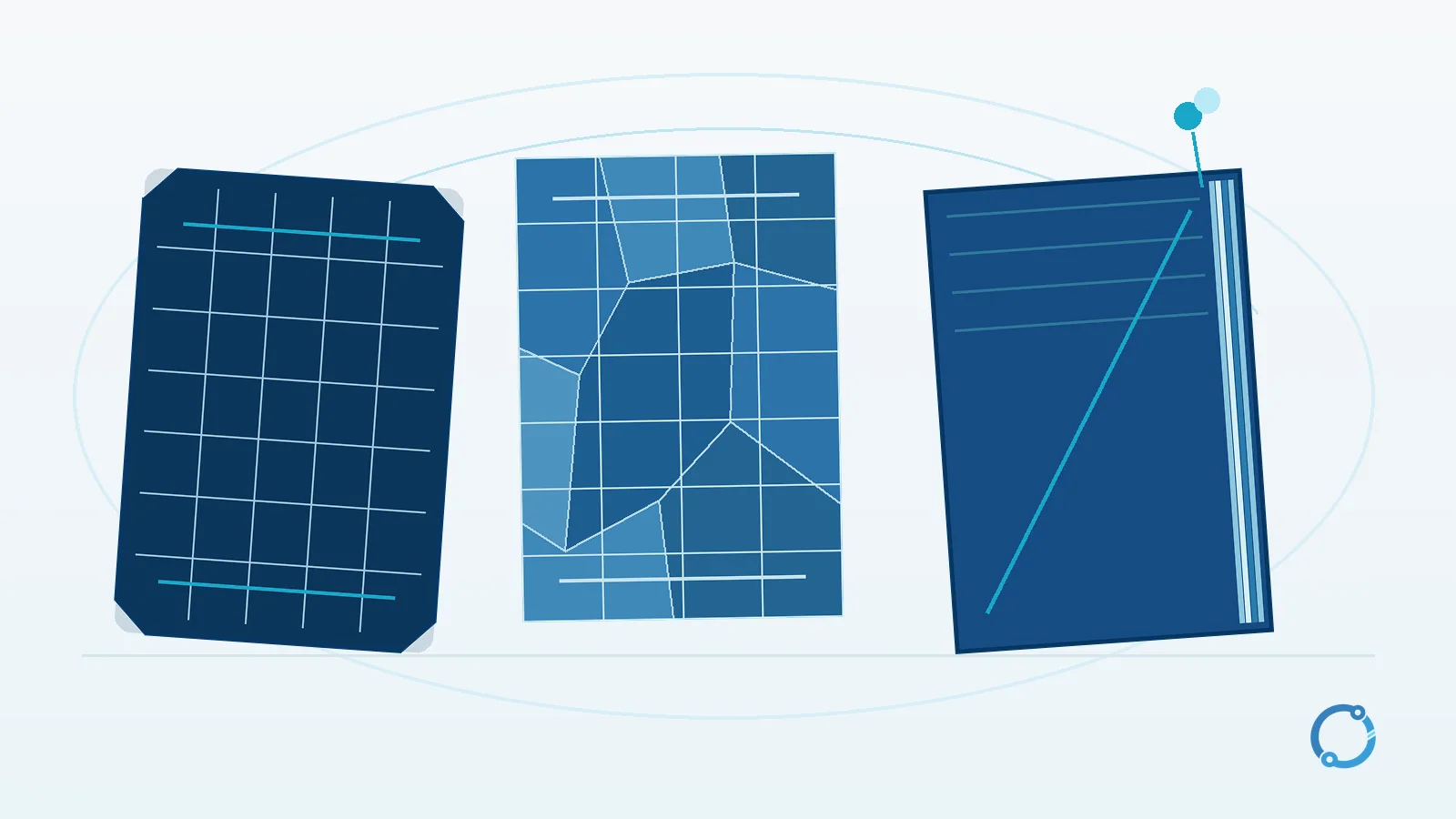
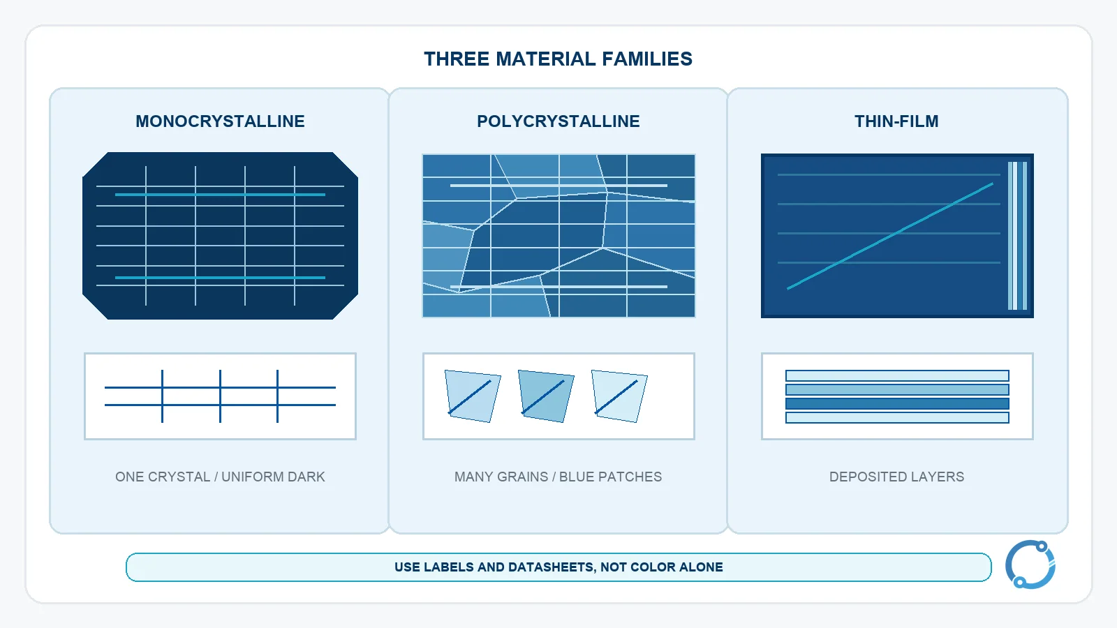
The solar panels sold for roofs, ground arrays and special surfaces are usually grouped into three material and structure families: monocrystalline silicon, polycrystalline silicon and thin-film. Monocrystalline cells are made from a single-crystal silicon wafer; polycrystalline cells contain many crystal grains; thin-film cells use one or more PV layers deposited on a supporting material.
The first practical distinction is efficiency position. Monocrystalline generally has the highest efficiency position, polycrystalline sits below it, and thin-film is generally below crystalline silicon. The second distinction is what fits the installation surface. Higher efficiency reduces the area needed for a given output, but it does not by itself guarantee a better annual energy result.
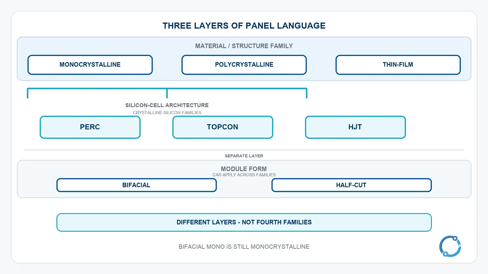
The title also mentions bifacial, but bifacial is not a fourth material family. It describes a module that can collect light on both sides. A bifacial monocrystalline module is still monocrystalline. The same logic applies to PERC, TOPCon, HJT and half-cut designs: they are architecture or module-form descriptions that sit at a different layer from the three families.
The classification map to keep in mind
The cleanest way to read the market is to separate three layers:
- Material and structure family: monocrystalline silicon, polycrystalline silicon and thin-film.
- Cell architecture: PERC, TOPCon and HJT are silicon-cell designs or process routes. They are not separate wafer-material families.
- Module form: bifacial and half-cut describe how cells are packaged or arranged in a module. They can be used with a family rather than replacing it.
This map prevents a common catalog-reading error. A listing may say “bifacial monocrystalline” or “half-cut TOPCon monocrystalline.” The words are not competing answers to the same question. The family is monocrystalline; bifacial and half-cut are module-form labels; TOPCon is a cell architecture.
Catalog language can also mix cell and module levels. A panel with monocrystalline cells may be framed as a full-size or half-cut module, and a bifacial package may use glass on both faces. Those are construction choices. The reader should keep the material family as the anchor and treat every other term as a modifier until the datasheet proves otherwise.
What efficiency means
Efficiency is the share of incoming solar power that a module converts into electrical output under stated test conditions. A simple area-based expression is:
output power = area x irradiance x efficiency
For a teaching comparison, use the standard test condition (STC) irradiance of 1,000 W/m2. The following example keeps the area and irradiance fixed so only efficiency changes:
10 m2 x 1,000 W/m2 x 0.20 = 2,000 W = 2.0 kW10 m2 x 1,000 W/m2 x 0.16 = 1,600 W = 1.6 kW10 m2 x 1,000 W/m2 x 0.12 = 1,200 W = 1.2 kW
A single panel example uses the same convention. A 2 m2 panel at 20% efficiency has a calculated STC output of approximately 400 W:
2 m2 x 1,000 W/m2 x 0.20 = 400 W
These are teaching values, not claims that every panel in a family has that efficiency. STC is a reference condition; real installations also experience temperature, irradiance, soiling, shading, wiring and conversion losses. The useful takeaway is narrower: for the same output, a lower-efficiency panel needs more surface area. That is why the first comparison column is efficiency position, while the selection decision still depends on the roof, mounting structure and actual product data.
Monocrystalline silicon
Monocrystalline silicon starts with a silicon ingot grown from a single crystal. Wafers cut from that ingot retain one continuous crystal structure. The DOE explains that monocrystalline silicon wafers are made up of one crystal structure, while polycrystalline silicon is made up of many different crystals. The ordered structure is the reason monocrystalline has the higher efficiency position.
The visible appearance is usually a uniform dark surface, often black or very dark blue. Wafers may have chamfered or rounded corners because of the shape of the grown ingot and the way the wafer is cut. That appearance is a useful identification clue, but it is not a proof of performance. Coatings, glass, framing and module design can change what a finished panel looks like.
Monocrystalline is the usual starting point when roof area is tight and the project needs more output per square meter. The DOE describes monocrystalline silicon as the most common absorber material in today’s solar modules and gives a current industrial-module benchmark of about 20%-22%. That benchmark is not a minimum, a warranty or a universal product rating. A buyer still needs the actual module datasheet, which should state the measured power, dimensions and test conditions.
Many monocrystalline products on the market use architecture variants such as PERC, TOPCon or HJT. Those names describe how the cell is designed and manufactured; they do not turn the product into a different material family.
Polycrystalline silicon
Polycrystalline silicon is cast from molten silicon into a block containing many crystal grains. The wafer therefore has grain boundaries: microscopic transitions between differently oriented crystal regions. Those boundaries interrupt the orderly crystal structure and help explain why polycrystalline generally sits below monocrystalline in the efficiency ranking.
The classic visual signature is a blue surface with visible crystalline patches or a fragmented grain pattern. Square wafers are common, although finished modules can hide the original wafer shape behind frames, busbars, glass texture and lighting. A blue, grainy appearance is a clue, not a laboratory test.
Polycrystalline has an important market boundary. The DOE currently describes monocrystalline as the most common absorber material in today’s solar modules, while the earlier PV Cells 101 explainer says monocrystalline and polycrystalline together account for almost all panels on the market. That does not mean the two families have equal current market weight. New module supply has moved strongly toward monocrystalline, and polycrystalline is increasingly encountered as remaining stock, lower-cost inventory or a legacy choice. It should not be presented as the default current mainstream option.
If a project is considering polycrystalline because the purchase price looks lower, compare the complete installed cost: mounting, area, wiring, labour, inverter compatibility and available warranty documentation all matter. The family name alone does not establish a financial advantage.
Thin-film
Thin-film PV is made by depositing one or more thin layers of photovoltaic material onto a support such as glass, plastic or metal. The DOE’s current cell-basics page lists cadmium telluride (CdTe) and copper indium gallium diselenide (CIGS) as the two main thin-film semiconductors on the market, and also discusses amorphous silicon as a thin-film route.
The three common thin-film examples have different engineering characters:
| Thin-film route | What it is | Visual and application notes |
|---|---|---|
| CdTe | A thin cadmium-telluride PV layer deposited on a support | Uniform dark panel; used at large-array scale; DOE notes that CdTe efficiency is generally below silicon |
| CIGS | A copper-indium-gallium-diselenide absorber layer | Uniform dark or dark-brown surface; can be deposited on flexible supports; manufacturing complexity is a key constraint |
| Amorphous silicon (a-Si) | A thin silicon layer with a non-crystalline structure | Lower efficiency position than crystalline silicon in common comparisons; used in niche or building-integrated products |
Thin-film can be flexible or lightweight when the product uses a flexible substrate, but that is a product-design result, not a property of every thin-film module. Some thin-film products have different low-light or temperature behaviour, but the direction and size of the difference vary by technology and datasheet. “Thin-film is better in heat” or “thin-film works better in shade” is too broad to use as a selection rule without module-specific evidence.
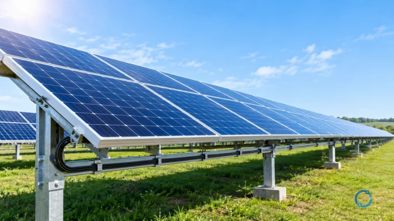
Thin-film is most relevant when the installation surface, weight limit, form factor or large-ground-array economics genuinely favour it. It is not automatically a residential-roof upgrade, and it is not a universal replacement for crystalline silicon.
Family comparison table
| Family | Cell material and structure | Appearance cue | Efficiency position | Relative cost position | Typical place in a project |
|---|---|---|---|---|---|
| Monocrystalline | Single-crystal silicon wafer | Dark, uniform surface; often chamfered corners | Higher; DOE industrial-module benchmark around 20%-22% | Usually the higher manufacturing-cost side of the DOE mono/poly contrast | Space-constrained roofs and projects that value output per area |
| Polycrystalline | Many silicon crystal grains | Blue, fragmented grain pattern; often square wafers | Lower than monocrystalline in the DOE comparison; no separate numeric range invented here | DOE describes lower manufacturing cost than monocrystalline | Remaining stock, budget-led projects and legacy replacements when verified as suitable |
| Thin-film | Deposited PV layer on glass, plastic or metal; CdTe, CIGS or a-Si | Uniform dark or dark-brown panel; construction depends on substrate | Generally below crystalline silicon in DOE comparisons; module datasheet controls | Different manufacturing and system-cost model; compare the complete installation | Large ground arrays and special surfaces where form, weight or scale justify it |
The table is deliberately conservative. DOE’s current pages support the direction of the efficiency comparison and a monocrystalline industrial benchmark, but they do not provide one universal current percentage range for every polycrystalline or thin-film product. Empty or qualitative cells are more honest than invented ranges.
The age of a product matters as well. A current monocrystalline module and an older polycrystalline module may both be in a warehouse, but they represent different generations of manufacturing. The comparison above describes family-level tendencies, not a guarantee that two specific panels from different years will rank in the same way.
PERC, TOPCon and HJT: architecture, not family
PERC stands for passivated emitter rear contact. The architecture adds backside passivation and local contact features so the cell can manage light and charge carriers more effectively than an older aluminum back-surface-field design. The DOE describes PERC as a design that overtook earlier Al-BSF cells because of its efficiency advantage. A PERC product is still a crystalline-silicon product.
TOPCon refers to tunnel-oxide passivated contacts. It is an n-type silicon-cell architecture that uses a thin passivation/contact stack to improve the backside interface. HJT, also described as silicon heterojunction (SHJ), combines crystalline silicon with thin amorphous-silicon layers to form a heterojunction. DOE describes the industry as moving from PERC toward n-type technologies such as TOPCon and silicon heterojunctions.
Those three names are useful when reading a module datasheet or a technology update. They are not the first branch of the family tree. The first question remains “which absorber family is this?” The architecture question comes next. A module can be described as monocrystalline TOPCon, monocrystalline HJT or another combination.
Bifacial and half-cut: form, not family
A bifacial module can collect light on its front and back. The backside may receive reflected light from the ground, roof or surrounding surfaces, so the possible contribution depends on albedo, mounting height, tilt, row spacing and the rest of the system design. DOE’s PV Cells 101 explainer notes that the effect of bifacial cells on system energy yield is still being quantified. That is why a bifacial label should not be translated into a guaranteed gain percentage.
A bifacial module can be monocrystalline, polycrystalline or thin-film depending on its actual construction. It is a package and system-integration choice, not a fourth material family.
Half-cut modules divide cells into smaller pieces and arrange the pieces in a different series-parallel pattern. The general intention is to reduce current per cell string and resistive loss while improving tolerance to some forms of mismatch. The exact electrical behaviour depends on the module layout and bypass-diode design. Half-cut is therefore a module-form description, not a new semiconductor family and not a promise of a fixed performance increase.
How to choose by project condition
Tight roof area
Start with monocrystalline, including its PERC, TOPCon or HJT variants. The higher efficiency position is most useful when the available surface cannot grow. Confirm the actual module dimensions and the inverter’s input window rather than relying on the family label alone.
Abundant area and a budget-led decision
Compare total installed cost rather than a single panel price. Polycrystalline may be available as remaining stock, but new-product availability can be limited. Verify the module’s datasheet, certification documentation and compatibility before assuming that the lower-cost label still holds. If the roof is large enough, the lower efficiency position may matter less, but the mounting and electrical design still have to be checked.
Large ground array or special surface
Thin-film deserves evaluation where its deposited form, flexible substrate, weight or large-area manufacturing route fits the project. CdTe and CIGS do not have identical characteristics, so the technology name is not a complete specification. The same principle applies to a-Si: use the actual product data and the intended application.
Bifacial or half-cut module
Consider bifacial only after checking the mounting geometry and reflected-light environment. Consider half-cut as a module-construction detail, not as a guaranteed upgrade. A module can combine a family, an architecture and a form; the labels should be read in that order.
Array sizing is a separate calculation. If the question is how many modules a house needs, use the dedicated guide to solar-panel count sizing. If the question is how the PV effect produces current, start with the solar-panel working principle. For system-level maximum-power tracking, the MPPT algorithms guide explains the control layer without changing the panel-family decision. The inverter explainer covers DC-to-AC conversion, and the battery article covers storage when the design includes a battery.
Frequently asked questions
Are monocrystalline panels always better than polycrystalline panels?
No universal “always” applies. Monocrystalline generally has the higher efficiency position, but a specific polycrystalline module can still be suitable when its measured performance, dimensions, availability and total installed cost fit the project. Compare datasheets and system requirements rather than the family name alone.
Is bifacial a fourth type of solar panel?
No. Bifacial describes a module that can collect light from both sides. It is a module-form layer that can sit on top of a monocrystalline, polycrystalline or thin-film product. The family remains the underlying cell material and structure.
Why do polycrystalline panels often look blue and fragmented?
Polycrystalline silicon contains many crystal grains, and the boundaries between those grains can produce a visible blue, patchy appearance. The look is an identification clue, not a guaranteed test of efficiency or quality.
Are thin-film panels suitable for a normal house?
They can be, but they are not the default choice for every roof. Thin-film may be attractive when a product’s flexible form, weight, large-area route or integration requirements fit the installation. Confirm the datasheet, mounting method and system compatibility before selecting it.
Does higher efficiency always mean more annual energy?
No. Higher efficiency can reduce the area needed for a given STC output, but annual energy also depends on irradiance, temperature, soiling, shading, orientation, inverter behaviour and system losses. Use the efficiency comparison to narrow the choices, then model the complete system.